• 5

中國人工智慧與半導體崛起:美國制裁失敗

China AI & Semiconductors Rise: US Sanctions Have Failed

https://www.semianalysis.com/p/china-ai-and-semiconductors-rise
9/12 撰文者 DYLAN PATEL, AFZAL AHMAD, 及 MYRON XIE

https://twitter.com/dylan522p DYLAN PATEL 是半導體業分析師 在 Twitter 有 2.7 萬個追隨者. 但根據回應顯然他是為匪宣傳

As we approach the 10 月 7日是中國製裁一週年
1-year anniversary on the October 7th China sanctions,之際,出口管制顯然正在失效。


拜登政府的既定目標是限制中國企業製造最高端晶片的能力,包括人工智慧和其他可能被中國共產黨用於邪惡目的的技術。請參閱下面美國的理由。 it is abundantly clear that the export controls are failing. The Biden Administration’s stated aim was to limit Chinese firms’ ability to manufacture the highest end chips including those in AI and other technologies that could be used for nefarious purposes by the Chinese Communist Party. See the US justification below.

中國正在快速發展百億億級超級運算能力,並宣布計劃在 2030 年成為人工智慧領域的世界領導者。The PRC is rapidly developing Exascale supercomputing capabilities and has announced its intent to become the world leader in AI by 2030.

中國正在使用這些系統進行軍事現代化,以提高其軍事決策、規劃和後勤以及自主軍事系統(例如用於認知電子戰、雷達、信號情報和乾擾。此外,中國正在使用這些先進的計算設備和「超級電腦」來改進武器設計和測試的計算,包括核武、高超音速和其他先進飛彈系統等大規模殺傷性武器的計算,並分析戰場效果。此外,中國正在使用先進的人工智慧監控工具,透過有效處理大量數據來實現監視、追蹤和監視公民等目的,而不顧基本人權。These systems are being used by the PRC for its military modernization efforts to improve the speed and accuracy of its military decision making, planning, and logistics, as well as of its autonomous military systems, such as those used for cognitive electronic warfare, radar, signals intelligence, and jamming. Furthermore, these advanced computing items and “supercomputers” are being used by the PRC to improve calculations in weapons design and testing including for WMD, such as nuclear weapons, hypersonics and other advanced missile systems, and to analyze battlefield effects. In addition, advanced AI surveillance tools, enabled by efficient processing of huge amounts of data, are being used by the PRC without regard for basic human rights to monitor, track, and surveil citizens, among other purposes.

限制中國獲得先進運算晶片或進一步開發人工智慧和「超級電腦」能力的能力,以用於違反美國國家安全和外交政策利益的用途。to limit the PRC's ability to obtain advanced computing chips or further develop AI and “supercomputer” capabilities for uses that are contrary to U.S. national security and foreign policy interests.

美國 2022 年 10 月限制US October 2022 Restrictions


然而,華為基於中芯國際N+2(7nm)製程的新旗艦晶片的發布,中國企業持續進口數十億美元的先進半導體製造設備,以及收購數十萬顆強大的NVIDIA H800&A800晶片,是However, the release of Huawei’s new flagship chip on SMIC’s N+2 (7nm) process, Chinese companies’ continued importation of billions of dollars of advanced semiconductor manufacturing equipment, and 非常acquisition of hundreds of thousands of powerful NVIDIA H800 & A800 chips明確的是,商務部製定的標準不會最終阻止中國突破去年秋天設定的壁壘。, it is abundantly clear that the Commerce Department’s standards were set at a level that will not ultimately inhibit China from breaking through the barriers set last fall.

在本報告中,我們將探討華為晶片對中國國內半導體製造和人工智慧能力軌跡的具體體現。我們將涵蓋:In this report we'll explore what the Huawei chip crystallizes about the trajectory of Chinese domestic semiconductor manufacturing and AI capabilities. We will be covering:

華為的晶片以及與國外晶片的競爭力。Huawei’s chip and its competitiveness with foreign chips.

華為內購晶片對蘋果、高通和聯發科的市佔率/平均售價/收入影響。The market share/ASP/revenue impact to Apple, Qualcomm, and MediaTek from Huawei’s insourcing of silicon.

中芯國際的N+2(7nm)製程技術、當前產能和擴展計劃SMIC’s N+2 (7nm) process technology, current capacity, and expansions plans

他們使用的光刻工具以及為什麼當前的限制是脆弱的。The lithography tools they use and why current restrictions are flimsy.

未來中芯國際5nm製程節點的潛力。The potential of a future SMIC 5nm process node.

使用 Nvidia 外部生產晶片的國內 AI 能力Domestic AI capabilities using externally produced chips from Nvidia

採用國內製造的AI晶片AI chips using domestic manufacturing

適用於無人機和偵測 F35 的 RF 功能RF capabilities for drones and detecting F35’s

最後,如果美國及其盟友對這一總體軌跡感到不安,西方可能對中國採取一系列與前端設備、化學品、先進封裝和智慧財產權許可相關的應對措施,這將完全將中共拒之門外。And finally, if the US and its allies are uncomfortable with this overall trajectory, a package of potential western responses to China related to front end equipment, chemicals, advanced packaging, and IP licensing that would totally shut out the CCP.
2023-09-25 21:40 發佈
華為麒麟9000S
Huawei Kirin 9000S


讓我們直接進入正題,由中芯國際生產的華為麒麟9000S。該晶片採用客製化的Armv9內核,以及華為設計的客製化GPU架構。能夠設計出中國領先的建築是一件大事。雖然美國過去曾阻止Let’s jump right in with the talk of the town, Huawei’s Kirin 9000S produced by SMIC. The chip uses a custom Armv9 core, and a custom GPU architecture designed by Huawei. The ability to design leading architecture in China is a big deal. While the US has stopped AMDAMD和 and 英特爾Intel與中國進行多項 CPU 交易,但在 Arm 方面卻未能做到這一點。部分原因是Arm在中國的合資企業 from various CPU deals with China in the past, it has not done been able to do so with Arm. Partially this is due to the joint venture Arm has in China, 不受其直接控制which is not under their direct control。另一個原因是Armv9指令集來自Arm Cambridge。此外,它們還使用 Arm 授權的 A510 核心。A510核心是在Arm的索菲亞法國研發中心+劍橋設計的。. Another reason is that the Armv9 instruction set is from Arm Cambridge. Additionally, they utilize Arm’s licensed A510 cores. The A510 core is designed in Arm’s Sophia France R&D center + Cambridge.

該晶片在技術上令人難以置信。The chip is technically incredible. The 各種測試中的性能和功耗概況performance and power consumption profile in a variety of tests使其與使用 1 至 2 年的高通晶片(S888 和 S8G1)相當。該晶片的射頻部分令人驚嘆,使用了與高通目前最好的整合式調變解調器相媲美的整合式調變解調器。這並不奇怪,因為華為在被禁止使用台積電之前領先高通。最重要的一點是,射頻前端晶片也是國產的,這是許多人認為中國缺乏的能力。 bring it on par with 1 to 2-year-old Qualcomm chips (S888 & S8G1). The RF side of the chip is amazing, using an integrated modem that is on par with Qualcomm’s current best. This is not surprising given Huawei was a bit ahead of Qualcomm before they were banned from using TSMC. The most important point is that the RF Front End chips are also domestically produced, which was a capability many thought China lacked.

最令人震驚的發現是,當在相同IP上進行直接比較時,The most shocking finding is that 華為麒麟9000S的Arm A510基於中芯國際的N+2(7nm)和2022年高通的S8G1基於三星的4LPX製程。when direct comparisons are done on identical IP, the Arm A510儘管存在工藝技術差距,Arm A510 核心的性能和功耗實際上彼此相當,這表明中芯國際 N+2 比西方大多數人意識到的要好。這些晶片彼此如此接近的部分原因是 for Huawei’s Kirin 9000S built on SMIC’s N+2 (7nm) and 2022 Qualcomm’s S8G1 built on Samsung’s 4LPX process. The performance and power consumption of the Arm A510 cores are effectively on par with each other despite the process technology gap, indicating SMIC N+2 is better than most in the west realize. Part of the reason these chips are so close to each other is 三星的良率較低Samsung’s poor yield,而中芯國際的 and SMIC’s good 良率較高yield。.

簡而言之,Kirin 9000S 的晶片設計比西方想像的更好。它具有堅實的動力和性能。即使出口管制乏善可陳,這也是一款領先的晶片,到 2021 年將接近領先地位,但它是在無法獲得 EUV、無法獲得美國尖端知識產權的情況下完成的,並且是故意受到阻礙的。我們無法誇大這是多麼可怕。Put simply, Kirin 9000S is a better designed chip than the West realizes. It has solid power and performance. Even with the lackluster export controls, this is a leading edge chip that would be near the front of the pack in 2021, yet was done with no access to EUV, no access to cutting edge US IP, and intentionally hampered. We cannot overstate how scary this is.

聯發科、高通和蘋果的影響MediaTek, Qualcomm, and Apple Impact
量化對蘋果的影響非常容易。由於2019 年底華為禁令的直接結果,他們的iPhone 銷量增加了約3500 至4500 萬部。對於蘋果來說,這很容易超過20B 美元的年收入,如果華為能夠重新站穩腳跟,這些收入可能會蒸發。這也只是智慧型手機,對蘋果來說,平板電腦、智慧手錶和筆記型電腦受到的影響會更大。Quantifying the impact to Apple is quite easy. They gained between ~35 to ~45 million units of iPhone sales as a direct result from the Huawei’s ban in late 2019. This is easily over $20B of annual revenue for Apple that could evaporate if Huawei is able to regain its old footing. That is just smartphones, the impact to tablets, smartwatches, and laptops will be even larger for Apple.

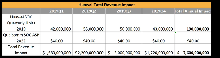
對聯發科和高通的影響更為嚴重。高通和聯發科是華為 SoC 年度 1.9 億顆的主要受益者,這些晶片在禁令後從市場上消失了。從2020年至今,這一份額轉移到了小米、Oppo和Vivo等其他中國廠商。如果華為恢復狀態,我們計算出對聯發科和高通的收入影響高達 $7.6B。The impact for MediaTek and Qualcomm is even worse. Qualcomm and MediaTek were the main beneficiaries of the 190 million annual Huawei SoC units that evaporated from the market following their ban. From 2020 to now, this share shifted to other Chinese vendors such as Xiaomi, Oppo, and Vivo. If Huawei regains its form, we calculate as much as $7.6B of revenue impact to MediaTek and Qualcomm.


當然,這是在14億支智慧型手機市場的情況. 現在的生產則還不到12億支。我們的客戶可以得到上述內容以及 RFFE 對 Skyworks、Qorvo、Murata、Qualcomm 和其他公司的影響進行更細緻的分析。This of course was in a 1.4 billion unit smartphone market, the current run rate is under 1.2 billion units. A much more nuanced analysis of the above as well as the RFFE impact to Skyworks, Qorvo, Murata, Qualcomm, and others is available for our clients

華為能否恢復狀態主要取決於中芯國際的製造能力,我們認為中芯國際的製造能力非常強大。The ability of Huawei to regain form hinges primarily on SMIC’s manufacturing capabilities, which we believe are very strong.
中芯國際N+2,真7nm,良率佳
SMIC N+2, A True 7nm, Good Yields


該製程從密度上來說是真正的7nm製程。雖然特定間距上的工程決策與台積電 2018 年的 7nm 不同,但應該被認為是類似的製程技術,而中芯國際最壞的情況也只是落後台積電幾年。有人可能會說,儘管受到限制,中芯國際最多只落後英特爾和三星幾年。由於中芯國際正在複製其他地方的做法,由於其來自中國大陸的優秀工程人才以及許多以前受僱於台積電的台灣移民,差距可能會進一步縮小。The process is a true 7nm process in terms of density. While the engineering decisions on specific pitches are different from TSMC’s 2018 7nm, it should be considered a similar process technology, and SMIC is at worst only a handful years behind TSMC. One could argue that SMIC is at most only a few years behind Intel and Samsung despite restrictions. As SMIC is replicating what has been done elsewhere, the gap could be even narrower due to their excellent engineering pool from mainland China as well as many courted immigrants from Taiwan that were formerly employed by TSMC.

如前所述,它在性能和功耗方面與三星的 4LPX 相當。最大的問題是As mentioned earlier it is on par with Samsung’s 4LPX in performance and power. The big questions are 產量yield和數量。雖然一些專家聲稱收益率僅為 10%,但我們並不相信這一點。事實上,我們認為中芯國際的工藝具有良好的良率。這裡沒有明確的數字,但有一些數據點表明了這一點。 and volume. While some pundits claim the yield is only 10%, we don’t believe that. In fact, we believe that SMIC’s process has good yield. There’s no definitive number here, but there are some data points that indicate this.

為什麼?我們從中國的消息來源聽到了一些溫和的評論,稱產量不錯。據稱他們的 D0 目前約為 0.14。作為參考,台積電的 N5 和 N6 節點大約是這個數字的一半。台積電當然是黃金標準,三星/英特爾的「7nm」更接近,但仍領先中芯國際。如此不錯的良率已經是中芯國際 N+2 製程技術健康發展的巨大標誌。參數產量是更重要、未知的指標。但道聽途說本身還不夠。Why? We’ve heard a few soft remarks from our sources in China that yield is good. Allegedly their D0 is currently about ~0.14. For reference, TSMC’s N5 and N6 nodes are about half that. TSMC of course is the gold standard, and Samsung/Intel “7nm” are closer although still ahead of what SMIC has achieved. Yield being this decent already is a huge flag that the SMIC N+2 process technology is healthy and developing. Parametric yield is the more important, unknown metric. But hearsay isn’t enough on its own.

更具體的證據是,FinFET 上的通道、閘極和汲極以及接點和下部金屬層看起來相當乾淨。低產量的製程可能看起來不那麼統一。For more tangible evidence, the channels, gates, and drains on the FinFETs as well as the contacts and lower metal layers look fairly clean. A process with low yield probably won't look as uniform. See these images from the 請參閱TechInsights公開簡報TechInsights 中的這些圖片。我們建議您查看他們的完整拆解,以獲取更多圖片和確切的推介。public brief. We recommend looking at their full teardown for more images and the exact pitches.

==

最後一個原因與晶片的明顯分檔有關。半導體製造中的「分箱」是指在製造和測試後根據積體電路(如 CPU 或 GPU)的性能和品質對積體電路(如 CPU 或 GPU)進行分類和分類的過程。雖然晶片可能存在有缺陷的電晶體(稱為災難性良率),但在許多情況下,工作電晶體仍然無法通過各種性能和功率測試。這稱為參數良率。如果一種製程技術的參數良率較低,那麼管理晶片良率的公司可以降低裝箱流程的嚴格性,以提高參數良率。更多的晶片可以通過各種測試,但也導致更高的可變性。The last reason is related to the apparent binning of the chip. "Binning" in semiconductor manufacturing refers to the process of sorting and categorizing integrated circuits (like CPUs or GPUs) based on their performance and quality after they have been manufactured and tested. While chips can have defective transistors, called catastrophic yield, in many cases, working transistors still fail various performance and power tests. This is known as parametric yield. If a process technology has low parametric yield, the firm managing yield for the chip can make the binning process less stringent to improve the parametric yield. More chips can pass various tests, but it also leads to higher variability.

這是在過去產量較低的行動晶片上實現的,例如三星 4LPX 上的高通 S8G1。以S8G1為例,在相同環境條件下,採用相同晶片的不同設備在完全熱浸設備上的差異可達10%以上。雖然我們還沒有在同一環境中對許多設備進行嚴格的測試,但各種中國論壇上的數據足以表明設備之間的差異相當低。This has been done with mobile chips that yielded poorly in the past, for example the Qualcomm S8G1 on Samsung’s 4LPX. In the case of the S8G1, different devices with the same chip would have differences upwards of 10% on fully heat soaked devices in the same environmental conditions. While we haven’t seen rigorous testing of many devices in the same environment, there is enough on various Chinese forums to show that device to device variation is quite low.

這些都不是萬能的,但我們相信中芯國際具有良好的良率,一些專家所說的10%的良率數字是無稽之談,旨在淡化其意義。這是真正的大批量生產流程技術。就像蘋果是台積電製程節點的白老鼠,幫助其提高產量並實現高良率一樣,華為也會以同樣的方式幫助中芯國際。None of this is bullet proof, but we believe that SMIC has good yield, and the 10% yield number some pundits have said is nonsense to downplay the significance. This is a real high volume production process technology. Just like Apple is the guinea pig for TSMC process nodes and helps them ramp and achieve high yield, Huawei will likewise help SMIC in the same way.

提醒一下,華為發布了As a reminder, Huawei released the 第一顆台積電N5生產的晶片first TSMC N5 produced chip,所以這是他們非常有能力扮演的角色。兩年內,中芯國際很可能能夠生產用於人工智慧和網路應用的大型單晶片。, so this is a role they are very capable of playing. In two years, SMIC will likely be able to produce large monolithic dies for AI and networking applications. This is a similar time scale to what 這與博通Broadcom和英偉達過渡到新製程技術的時間尺度相似。 and Nvidia’s transition to new process technologies.
中芯國際設備及工裝
SMIC Equipment and Tooling


這是因為他們能夠有效地使用台積電和英特爾在“7nm”製程中使用的所有相同工具。雖然理論上存在工具限制,但This is due to their ability to use effectively all the same tools that TSMC and Intel have access to for their “7nm” processes. While theoretically there are tooling restrictions, 看看我們去年對美國晶片製裁的深入研究see our deep dive into the US chip sanctions last year,它們實際上毫無意義。, they are effectively meaningless.

儘管中芯國際的N+1製程技術已經違反制裁規定,美國仍繼續向使用美國技術的半導體製造設備公司發放許可證。中芯國際、長鑫儲存以及許多其他直接與解放軍合作並追求超越制裁的工藝技術的中國公司繼續進口他們需要的任何工具。實際上沒有任何禁令,國際清算銀行和國務院的最終用途檢查也失敗了。Despite SMIC’s N+1 process technology already violating sanctions, the US continued to grant licenses to semiconductor manufacturing equipment firms utilizing US technology. SMIC, CXMT, and many other Chinese companies that work directly with the PLA and are pursing process technologies that exceed sanctions continue to import whatever tools they need. There are effectively no bans and end use checks from the BIS and State Department are failing.

應用材料公司、泛林集團、東京電子、KLA、Screen、ASM International、Kokusai等設備公司基本上都在向中國銷售他們提供的所有工具。這是因為大多數7nm甚至5nm的沉積、蝕刻、計量、清潔、鍍膜機、顯影器、離子注入、外延等工具也可以在28nm中使用。這些工具以「28nm」的價格出售給中芯國際,但實際上,中芯國際正在向企業撒謊,並將其用於7nm。The equipment companies such as Applied Materials, Lam Research, Tokyo Electron, KLA, Screen, ASM International, Kokusai, etc. are selling basically every tool they offer to China. This is because most deposition, etch, metrology, cleaning, coaters, developers, ion implant, epitaxy, etc. tools for 7nm and even 5nm can also plausibly be used in 28nm. These tools are being sold to SMIC for “28nm,” but, in reality, SMIC is lying to the firms faces and using them for 7nm.

雖然中芯國際正在擴展 28 奈米和其他後沿節點,但其規模遠小於他們聲稱的,因為這些工具正在重新繞道使用在前端技術。這些設備公司內部的人員甚至有可能知道正在發生的事情,卻視而不見。While SMIC is expanding 28nm and other trailing edge nodes, it is much less than they claim as these tools are being rerouted to leading edge. It’s even possible that people within these equipment firms know what’s happening, but are turning a blind eye.

出口管制失敗了。這些規定沒有執行,現狀依然如此。The export controls are failing. They are not being enforced and the status quo has continued.
光刻設備 Lithography Equipment

光刻世界與其他工具有些不同。現在雖然對於特定的 DUV 工具有一些限制, 問題是它們對於阻止7nm毫無意義。
The lithography world is a bit different than the rest of these tools. There are some restrictions on specific DUV tools. The problem is they are meaningless for preventing 7nm. 我們在一月份詳細討論過這些問題We spoke through the problems in detail back in January,但讓我們簡單回顧一下。, but let’s rehash briefly.

中國能夠並且將能夠利用目前允許的光刻工具提高 7nm 的產量。NXT:1980i 以及改進的 Di、Ei 和 Fi 工具可以在當前限制下匯入和維護。最初的 1980i 是台積電用來以極高的良率將其 N7 (7nm) 每月生產超過 100,000 片晶圓的工具。1980i 系列也被英特爾用於「7nm」。China can and will be able to ramp 7nm production with currently allowed lithography tools. The NXT: 1980i, and improved Di, Ei, and Fi tools can be imported and serviced under current restrictions. The original 1980i is the tool TSMC used to ramp their N7 (7nm) to over 100,000 wafers a month at very high yield. The 1980i series was also used by Intel for their “7nm.”

任何熟悉該領域的人都清楚這個漏洞。這是無效政策的完美例子,其既定目標是阻止進一步發展,同時為中國濫用留下了明顯的漏洞。ASML 繼續受益並計劃大幅增加 DUV,主要由這些「舊」工具帶動。This loophole has been clear to anyone whose familiar with the space. This is a perfect example of ineffective policy, whose stated goal is to stop further development, while leaving a clear loophole for China to abuse. ASML continues to benefit and plan for a massive increase in DUV, mostly lead by these "older" tools.

中芯國際產能不受限
SMIC Capacity Is Not Limited


而中芯國際7nm製程有超過60層光刻。其中只有大約 40 個是關鍵層,但為了後代的緣故,我們只說 60 個層需要最新的 1980 工具。事實上,較舊的 ArFi 工具(來自 Nikon 和 ArF/KrF/I-Line 等供應商的工具)可用於許多此類層。While there are over 60 layers of lithography in the SMIC 7nm process. Only about 40 of these are critical layers, but for posterities sake let’s just say 60 layers require the latest 1980 tools. In reality, older ArFi tools, those from vendors like Nikon, and ArF/KrF/I-Line can be used for a number of these layers.

ASML 聲稱最新的 1980Fi 每小時可以進行 330 層光刻,但我們認為這有點樂觀,並且是根據低劑量計算的。讓我們保守一點,假設ASML claims the latest 1980Fi can do 330 layers of lithography an hour, but we believe this is a bit optimistic and is calculated off a low dose. Let’s be conservative and say 中芯國際使用的劑量是 ASML 聲稱的兩倍SMIC uses 2x the dose that ASML claims,而且他們擁有一支 Di 艦隊,而不是 Fi。這意味著每個工具每小時可以處理約 165 層。 plus they have a fleet of Di, not Fi. This would mean each tool could do ~165 layers per hour.

我們聽說中芯國際擁有超過 30 種來自 ASML 的先進 ArFi 工具。他們還訂購了更多光刻工具,包括最新的 1980Fi。這些工具支援所有製程節點,但可用於 7nm 和 5nm。我們還聽說他們的第一座 7nm 晶圓廠將擁有總共 15 個 ArFi 工具,該工廠將於 2024 年第二季末完全配備。此後還需要幾個季度的時間才能實現產能提升。有傳言說他們的下一個晶圓廠將會更大。來自中國的更多傳言稱,第一座晶圓廠將每月生產 5 萬片 7 奈米晶圓(WPM),但我們第一次聽到這個消息時,最初似乎太大了。We hear SMIC has well over 30 advanced ArFi tools from ASML. They have many more lithography tools on order as well, including the latest 1980Fi. These tools support all their process nodes, but can be used for 7nm and 5nm. We also hear they will have 15 total ArFi tools for their first 7nm fab which will be fully populated by the end of Q2 2024. It will take a few more quarters to ramp after that. Rumors state their next fab will be even larger. More rumors from China claim the first fab will have 50k wafers per month (WPM) of 7nm, but that initially seemed too big the first time we heard of it.

雖然我們無法驗證中國的這些說法,但中芯國際似乎很容易在其 7nm 晶圓廠中將實際產量提高到 30k WPM,而無需從其他後緣晶圓廠獲取工具。While we can’t validate these claims from China, it does appear to be very easy for SMIC to get ramp to 30k WPM of actual production in their 7nm fab, without taking tools from other trailing edge fabs.


如果他們能夠將 1980i 所需的層數減少到 50 並且他們使用的劑量更接近 ASML 聲稱的劑量,那麼這與樂觀的 50k WPM 聲稱相符。This tacks with the optimistic 50k WPM claims, if they can bring the number of layers requiring 1980i down to 50 and they use doses closer to ASML claimed doses.

即使良率達到 50%,30,000 WPM 每年仍可支援超過 1,000 萬個 Nvidia H100 GPU ASIC 晶片。Even with 50% yields, 30,000 WPM could support over 10 million Nvidia H100 GPU ASIC dies a year. 目前,用於先進封裝(類似於 CoWoS或高頻寬記憶體 (HBM))的裝置也沒有受到限制。No equipment就容量而言,貓已經洩露了秘密。 used for advanced packaging similar to CoWoS or High Bandwidth Memory (HBM) is currently limited either. The cat is already out the bag in terms of capacity.
5奈米是可能的
5nm Is Possible


ASML 每年將增加 400 多個 ArFi 工具的出貨量,ASML is ramping to ship over 400 ArFi tools a year, 並聲稱到 2025 年將達到 600 個 DUV 工具的產能with claims of hitting 600 DUV tool capacity by 2025。超過一半的產能是為了滿足他們認為來自中國晶圓廠的需求。雖然這些工具將廣泛分發給許多公司,但中芯國際是 ASML 在中國最大的個人客戶。. More than half of the capacity is penned for demand they see coming from Chinese fabs. While these tools will be distributed widely, to many companies, SMIC is the largest individual customer for ASML in China.

ASML 公開表示,到 2030 年,每月將有超過 150 萬片過剩/低效晶圓ASML openly says this is explicitly for over 1.5 million excess/inefficient wafers per month by 2030,每年還會額外增加 15 萬 WPM 的過剩/低效產能。ASML表示這是由於, with an additional 150k WPM of excess/inefficient capacity added each year. ASML says this is due to 半導體供應鏈的區域化regionalization of semiconductor supply chains,但這只是, but that’s just a cover for 中國實現半導體獨立China achieving semiconductor independence並利用DUV達到5奈米的幌子。 and using DUV to reach 5nm.

需要非常明確的是,ASML 的產能計畫中明確包含了這一點,並To be abundantly clear, it is 根據最後一個投資者日預測,從半導體製造的角度來看,中國將實現半導體獨立explicitly built into ASML’s capacity plans and forecasts that China will be semiconductor independent。當然,供應鏈的其餘部分仍然高度交織,包括設備、消耗品和設計智慧財產權。 from a semiconductor fabrication standpoint as per their last investor day. The rest of the supply chain is of course still highly intertwined including equipment, consumables, and design IP.

ASML 與 2025 年和 2030 年的半導體市場
ASML 與 2025 年和 2030 年的半導體市場ASML & The Semiconductor Market In 2025 & 2030
迪倫·帕特爾DYLAN PATEL
··
2022 年 11 月 22 日NOVEMBER 22, 2022
閱讀全文Read full story
使用 ArFi 多重圖案化可以實現每 mm^2 超過 1.3 億個電晶體的「5nm」工藝,並實現高產量。A “5nm” process that achieves over 130 million transistors per mm^2 is possible to achieve with high yields using ArFi multi-patterning. 1980i 系列的覆蓋能力足夠好,可以以可接受的良率製造 5nm。The overlay capabilities of the 1980i series is good enough that 5nm can be manufactured at acceptable yields.

考慮到政府補貼的水平,中芯國際 N+3「5nm」製程的生產也很經濟。雖然我們估計,缺乏 EUV 會使總光刻成本增加 55% 至 60%,但請記住,This SMIC N+3 “5nm” process would also be economical to produce given the level of governmental subsidies. While the lack of EUV would increase total lithography costs by 55% to 60% in our estimation, remember that 目前 5nm光刻成本僅佔總製程成本的 30% 左右。lithography is only ~30% of the total process cost這意味著總製程成本僅比採用 EUV 的 5 奈米高出約 20%。良率可能會受到影響,因此由於每片晶圓的缺陷晶片更多,實際數量會更高,但這對中國來說不會是不可逾越的障礙。 at 5nm currently. This means that the total process cost would only be ~20% higher versus a 5nm that utilizes EUV. Yield likely takes a hit and therefore the actual number will be higher due to more defective chips per wafer, but it will not be an insurmountable barrier for China.

如果目前的限制沒有改變,我們預計華為和中芯國際將在 2025 年或 2026 年推出真正的基於 5 奈米的晶片,並在不久之後推出大規模人工智慧晶片。目前的出口管制並沒有限制中國的製造能力或產能。If nothing changes with current restrictions, we expect Huawei and SMIC to have a true 5nm based chip in 2025 or 2026 with large scale AI chips not so long after. The current export controls are not limiting China’s manufacturing capabilities or capacity.
中國人工智慧能力
China AI Capabilities


製造能力並非遙不可及,但即使沒有這些國內製造能力,中國的人工智慧能力也將極為強大。到2024年底,中國將總共擁有超過100萬顆Nvidia A100或更好的晶片。請記住,Manufacturing capabilities are not out of reach, but even without those domestic manufacturing capabilities, China’s AI capabilities will be extremely strong. By the end of 2024, China in total will have more than 1 million A100 caliber or better chips from Nvidia. Remember GPT-4 是在約 24,000 個GPT-4 was trained on ~24,000A100 上進行訓練的, A100’s and 即使到明年年底,Open AI 仍將擁有不到 100 萬個高級 GPU Open AI will still have less than 1 million advanced GPUs even by the end of next year。.

目前對人工智慧的限制充其量是脆弱的。Nvidia 很快就推出了 A100 和 H100 GPU 的新版本,它們的功能實際上與 A800 和 H800 相同。這些 GPU 不會減少總運算或記憶體頻寬。雖然 NVLink 速度降低至 400GB/s,但這對於所採用的大多數平行策略(例如 8x 張量並行、完全分片資料並行和管道並行)並沒有限制。這些削減也無法進行最終用途檢查,並且如果硬體沒有被熔斷,則可能會像 Nvidia 以前的加密採礦限制器一樣被逆轉。The current restrictions on AI are flimsy at best. Nvidia quickly made new versions of their A100 and H100 GPUs that are effectively just as capable named the A800 and H800. These GPUs do not cut down the total compute or memory bandwidth. While NVLink speed are cut to 400GB/s, that is not restrictive for most parallelism strategies that are employed such as 8x Tensor Parallel, Fully Sharded Data Parallel, and Pipeline Parallelism. These cut downs are not able to be end use checked either and could potentially be reversed like Nvidia’s former crypto mining limiters, if the HW isn't fused off.

此外,對於部署了數萬個 H100 GPU 的最高端系統,它們僅使用 50GB/s 的乙太網路/Infiniband IO 從每個 GPU 到每個伺服器外部網路上的其他 GPU。限制的標準是晶片到晶片 IO 總量為 600GB/s。比 H100 更好的晶片可以在外部製造並在當前有缺陷的製裁下合法進口。例如,理論上的 3nm 晶片,其 FLOPS 是 H100 的 10 倍,記憶體頻寬是 H100 的 5 倍,乙太網路/超乙太網路/Infiniband 速度為 500GB/s,在目前限制下可以進口。在當前限制下可以進口晶圓級晶片/封裝。Furthermore, for the highest end systems with tens of thousands of H100 GPUs being deployed, they only use 50GB/s of Ethernet/Infiniband IO from each GPU to other GPUs on the network outside of each server. The bar for the restriction is 600GB/s total chip to chip IO. Chips better than the H100 can be made externally and imported legally with the current flawed sanctions. For example a theoretical 3nm chip with 10x the FLOPS of H100, 5x the memory bandwidth, and 500GB/s of Ethernet/Ultra Ethernet/Infiniband can be imported under current restrictions. A wafer scale chip/package can be imported under current restrictions.

中國將擁有西方公司的尖端晶片,並且很快就能訓練 GPT-4 和更好的同等產品。China will have cutting edge chips from western firms and will be capable of training GPT-4 and better equivalents soon.
國產AI晶片能力
Domestic AI Chip Capabilities

許多規模化企業和人工智慧硬體新創公司很快就能提供與 Nvidia A100 相當的晶片。其中包括華為、必人、騰訊、阿里巴巴、百度、MetaX 等。雖然我們今天不會深入探討他們的所有能力,但他們將能夠在 2 年內輕鬆地以中芯國際 7 奈米技術大批量交付 A100 級晶片。雖然軟體是一個挑戰,但中國的軟體開發商比美國、加拿大和歐洲的總和還要多。這也不應該是一個無法克服的挑戰。There are many scaled players and AI hardware startups that will soon be able to deliver on chips that are on par with Nvidia’s A100. These include Huawei, Biren, Tencent, Alibaba, Baidu, MetaX, and more. While we won’t dive into all their capabilities today, they will easily be able to deliver A100 class chips on SMIC 7nm in 2 years at significant volumes. While software is a challenge, China has more software developers than the US, Canada, and Europe combined. This shouldn’t be an insurmountable challenge either.

這些晶片大多使用 Cadence、Synopsys 和 Mentor Graphics(西門子)的美國 EDA IP 進行設計。These chips are mostly designed using US EDA IP from Cadence, Synopsys, and Mentor Graphics (Siemens). 華為正透過大規模投資快速推進國內EDA。Huawei is rapidly advancing domestic EDA by investing massively.像 MetaX 這樣的一些廠商公然抄襲 Nvidia Some players like MetaX are blatantly copying Nvidia ,使他們的晶片相容於 CUDA by making their chips CUDA compatible。像Biren這樣的公司有很多來自Nvidia上海的設計師,. Others like Biren have many designers from Nvidia Shanghai and 他們的架構如果你瞇著眼睛看的話很容易讓人想起Nvidia的their architecture is very reminiscent of Nvidia’s if you squint your eyes,, and 這是一個很好的架構it’s a good architecture。Biren 已經. Biren has already 試圖逃避我們獨家透露的製裁。attempted to evade sanctions which we revealed exclusively.

微架構和系統設計將會不斷發展,憑藉中國國內的半導體製造能力,比H100更好的晶片已經指日可待。中國Microarchitectures and system design will evolve and chips better than the H100 are well within sight with China’s domestic semiconductor manufacturing capabilities. China is 有能力建造超大型超級電腦並將其聯網。capable of building and networking very large supercomputers together.此外,中國擁有領先的光學製造能力,擁有像旭創這樣的公司。先進封裝也正在迅速發展。先進封裝和光學的結合將使中國即使被限制在5奈米或7奈米製程技術上,也能與國產半導體保持競爭力。 Furthermore, China has leading optics manufacturing capabilities with firms like Innolight. Advanced packaging is also being developed rapidly. The combination of advanced packaging and optics will enable China to remain competitive with domestically produced semiconductors even if they are held back to 5nm or 7nm process technology.

光是明年,中國就會有多家公司能夠提供比 GPT-4 更好的培訓。這甚至不是一個問題。中國可能比西方更有效地將 法學碩士 LLM 大型語言模型 武器化,因為中國軍民融合,而且缺乏陳舊、緩慢且極其昂貴的現有國防工業,就像他們在無人機方面所做的那樣。China will have multiple firms capable of training better than GPT-4 next year alone. It’s not even a question. China is probably able to more effectively weaponize LLMs than the west is too due to their civil-military fusion and lack of antiquated, slow, and extremely expensive existing defense industry, just like they have with drones.
sroach

最後一段的 LLMs 應該翻譯成 "大型語言模型",不是法學碩士啦 XD,當然把律師用投石機丟出去的確是可以當武器用 [茶]

2023-09-26 9:53
maya95
maya95 樓主

sroach 保留原文的好處, 文章太長我也沒全看[^++^]

2023-09-26 11:25
無線電和感測器
Radio And Sensors

順便說一句,除了對無線電/感測器功能進行一些輕微無效的製裁之外,實際上沒有採取任何措施。通訊和感測器技術對於戰爭來說是最重要的,至少在歷史上是如此。雖然隨著無人機使用的快速增加,這種情況可能會發生變化,但最有效的無人機正在有效地使用看起來很像手機硬體的硬體。此外,中國已經擁有能夠偵測F-35的雷達。As an aside, there is practically nothing being done besides some minor ineffective sanctions on radio/sensor capabilities. Communications and sensors technologies are the most important for war, at least historically. While this may be changing with the rapid increase in drone use, the most effective drones are effectively using hardware that looks a lot like phone hardware. Furthermore, China already has radars capable of detecting the F-35.

他們繼續利用各種先進的化合物半導體來改進這一點。為國內碳化矽和氮化鎵工業進口的設備也被用於在戰爭中有用的射頻應用。此外,還有多家公司,如意法半導體(其技術為SpaceX Starlink的核心技術),正在積極合作並They continue to improve this with various advanced compound semiconductors. The equipment being imported for their domestic silicon carbide and gallium nitride industries is also being used for RF applications that will be useful in war. Furthermore, there are multiple firms such as STMicroelectronics, whose technology is core to SpaceX Starlink, who are actively collaborating and 進行JV/IP轉移doing JV/IP transfers。.

該合資企業/智慧財產權將極大地加速中國的能力,其幌子是該技術只能用於功率半導體應用,儘管從合資企業獲得的所述技術能力相對容易重新用於射頻應用。This JV/IP that will accelerate China’s capabilities massively under the guise that the technology can only be used for power semiconductor applications despite relatively easy repurposing of said technology capabilities gained from the JV for RF applications.

可以做什麼What Can Be Done
美國政府明確認為,中國半導體產業能夠生產 14 奈米以下晶片以及 128 層或以上 NAND 和 18 奈米半節距或以下 DRAM 儲存 IC,對全球安全構成重大威脅(請參閱此處的開源報告) 。承擔The US government clearly views a Chinese semiconductor industry that can produce sub-14nm chips and memory ICs with 128 layers or more for NAND and 18nm half-pitch or less for DRAM as a significant threat to global security (解放軍打算用人工智慧晶片做的事情see here for an open-source take on what the PLA intends to do with AI chips)。維持目前的出口管制水準對美國及其盟國的長期經濟和國家安全構成重大威脅。). Maintaining the current level export controls poses a significant threat to America and its allies’ long-term economic and national security.

美國政府及其盟友可能會阻止中國半導體產業的發展。以下是可以採取的一些措施,以確保中國在未來幾年不會發展出大規模製造高端軍事應用所需晶片的能力:The US government and its allies could stop the Chinese semiconductor industry in its tracks. Here are some steps that could be taken to ensure that China does not develop the ability to mass-manufacture the sorts of chips needed for high-end military applications in the coming years:

  • 限制 ArFi 浸沒式微影工具。Limit ArFi immersion lithography tools.
  • 限制現有設備的維修。Limit servicing of existing equipment.
  • 限制ArFi光阻。Limit ArFi photoresist.
  • 限制光罩。Limit masks.
  • 限制掩模空白、寫入器和其他相關基礎設施。Limit mask blanks, writers, and other associated infrastructure.
  • 限制計量設備。Limit metrology equipment.
  • 限制 CMP 設備。Limit CMP equipment.
  • 限制外延設備。Limit epitaxy equipment.
  • 限制乾蝕刻設備。Limit dry etch equipment.
  • 限制 CVD 和 ALD 設備。Limit CVD and ALD equipment.
  • 限制先進的包裝設備。Limit advanced packaging equipment.
  • 限制離子注入設備。Limit ion implantation equipment.
  • 限制半導體製造設備子系統和組件。Limit semiconductor manufacturing equipment subsystems and subassemblies.
  • 限制蝕刻劑氣體。Limit etchant gas.
  • 限制沉積前驅物。Limit deposition precursors.
  • 限制具有 >25.6Tbps IO 的晶片,即使它們沒有計算。Limit chips that have >25.6Tbps of IO even if they have no compute.
  • 限制效能 >1000TOPS 的晶片。Limit chips that have >1000TOPS of performance.
  • 限制Limit the 200G SerDes的許可licensing of 200G SerDes。.
  • 限制 EDA 工具。Limit EDA tools.
  • 限制合資企業和境內投資。Limit Joint Ventures and inbound investments.

只做一半是行不通的,但全面進攻將使在中國國內複製半導體供應鏈的成本幾乎不可能。雖然我們沒有具體提倡其中任何一項,但很明顯,如果採取果斷行動,西方仍然可以阻止中國的崛起。Half measures will not work, but a full-scale assault will make it so the cost of replicating the semiconductor supply chain domestically is neigh on impossible. While we aren’t advocating for any of these specifically, it is clear the west can still stop China’s rise if decisive action is taken.
以上是 SemiAnalysis 對中國半導體業現況的分析.

自己解讀

====

Patel 今年才參觀台積電第12 廠

說這裡是全世界最重要的地方

原來他是被中國雇用寫這篇文章為匪宣傳

https://finance.ettoday.net/news/2498959

記者廖婕妤/台北報導

護國神山台積電(2330)在全球的地位舉足輕重,半導體研究公司SemiAnalysis首席分析師Dylan Patel今(14)日在推特上分享一連串他「騎車繞台積電Fab 12」的照片,直言在台積電附近晃踏「沒有人阻止我」,附近工作的工人甚至向他招手,而他也用翻譯軟體表達「這是地球上最重要的地方,你做得很棒。」

Dylan Patel是半導體分析師,對產業研究與諮詢有一定認知,而他騎自行車繞行台積電廠區時也觀察了台積電開發7奈米、5奈米和3奈米產品的地方。
  • 5
內文搜尋
X
評分
評分
複製連結
Mobile01提醒您
您目前瀏覽的是行動版網頁
是否切換到電腦版網頁呢?