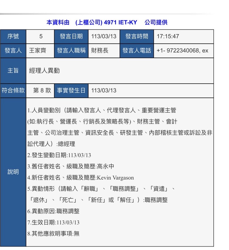


原先預測股價會到168元.
想縮美國會給5億挹注EPS.
如今沒達標.只好認錯發懺悔文.
偶已出清英特磊.改買以下這檔股票.
所以不要再私我問何時會到預估價嘞啦.
重申目標價不變....只是偶沒哪麼多美國時間等QQ..
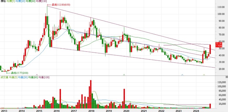
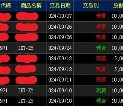
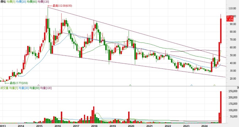
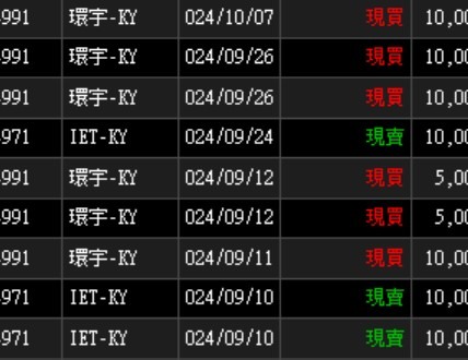
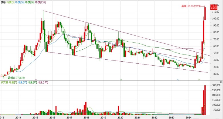
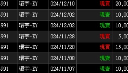


 九月怒買環宇-ky(4991)的理由

1.買進時預期連續假虧15季後.即將首度轉虧為盈.會產生猛爆型的股價反彈.
(為啥是假虧呢..以業外認列虧損最多的常州承芯來說.表面每季認列高達1塊多eps虧損.
其實持有2成承芯持股未上市估值驚人.潛在淨獲利高達5倍環宇母公司本體股本.
隨便賣個1%持股就能當季轉虧為盈)
2.美國議員提議要封殺.在美國及全世界市占超過6成的大陸光模塊巨嬰廠商.
有利美國本土廠.環宇自有品牌KGD光模組搶市.填補6成市場空缺坐大.
3.美國光通訊大廠麥威爾預告2025年1月1日全面調漲光通訊產品報價.
讓環宇直接受惠.擠身2025年漲價概念股.
4.投信圈傳出繼上詮獲台GG獨家認證cpo關鍵廠後.環宇將成台積電CPO二極體晶粒供應商.
遭各家投信鎖定作帳.坐等台GG公布光收發晶粒獨家認證後收割.爭奪2025年績效分紅.
5.全世界只有博通和環宇有能力做出1.6T光模組所需的200G-PD晶粒.當明年進入3.2T
光模組後.環宇800G產能過半+1.6T大量供貨+3.2T試產.而其他400G量產800G試產的台廠
直接失去競爭力掛掉.台積電腳踏兩條船全包了.跟輝達博通聯手設計.再跟環宇拿光晶粒封裝.
6.環宇機台借台積電(2330)秘密測試
 實驗多年.檯面下合作緊密.拉抬環宇CPO光通訊地位
抗衡博通獨大的風險有其必要性.(作法如當年拉抬家登3680-擊潰國際光罩盒大廠如出一策)
7.川普凍蒜了.美國優先.英特磊和環宇是台股唯二2家.純美國公司+AI概念股.
而環宇在最火熱的2025年光通訊產業中.營收比又高達6成以上.完封英特磊.
所以砍英買環.坐等川普1月上台後市場再度熱炒美國優先受惠+光通訊漲價概念股
DARPA awards University of Michigan’s Zetian Mi $3m to scale III–V materials on silicon
The project ‘CMOS compatible, defect-free universal growth of III–N and III–V multilayer heterostructures on Si (001)’ of Zetian Mi, professor of Electrical Engineering and Computer Science in the University of Michigan’s Department of Electrical and Computer Engineering (ECE), has been awarded $3m by the US Defense Advanced Research Projects Agency (DARPA) as part of its Material Synthesis Technologies for Universal and Diverse Integration Opportunities (M-STUDIO) initiative. The goal of M-STUDIO is to “realize a universal heterogeneous integration technology, compatible with leading-edge and future advanced-node semiconductor manufacturing processes, via atomic-precision nano-scale multi-layer material synthesis”.
Zetian Mi. (Photo: Brenda Ahearn, Michigan Engineering.) Picture: Zetian Mi. (Photo: Brenda Ahearn, Michigan Engineering.)
To achieve this goal, Mi and his collaborators Kai Sun (of the University of Michigan’s Department of Materials Science and Engineering) and Patrick Fay (of University of Notre Dame) will use a new method to grow ultra-thin layers of III–V compound semiconductor crystals without a foreign metal catalyst, which often introduces impurities. These tens-of-atoms thick layers will allow Mi’s team to grow the semiconductor materials on a silicon lattice without defects.
The final goal of the project will be to partner with Intelligent Epitaxy Technology Inc (IntelliEPI) of Richardson, TX, USA – which manufactures MBE-grown epitaxial wafers – to show the viability of this material at scale for use in industry.
“We must find new materials that have fundamentally better properties than silicon, as far as transistor functionality, but they need to be integrated into the current manufacturing processes,” says Mi. “It’s not likely for the industry to give up many billions of dollars of infrastructure. As such, the new material should ideally be CMOS compatible,” he adds.
“We are looking into the fundamental, long-standing challenge of integrating compound semiconductors with silicon,” says Mi. “It’s a very difficult problem, but if we are successful, there is the possibility that this material will go into every computer, every cell phone, virtually every electronic device that we use.”
內文搜尋
X

