gamli wrote:謝謝補充資訊,以下是我直接剪貼到google的翻譯。
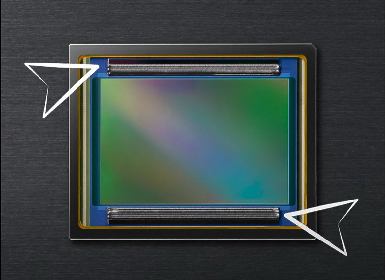
partially stacked cmos
只在CMOS上面和下面的區塊塞入stacked 線路, 每想到還可以這樣的方式設計CMOS...也算是節省成本
這樣的CMOS設計就看之後的測試報告, 真的有意思
https://www.theverge.com/2024/6/17/24178637/nikons-new-2500-z6-iii-has-the-worlds-first-partially-stacked-cmos-sensor
This is the first camera ever to employ this technology. Instead of the circuit parts and pixel area both stretching the full corner-to-corner dimensions of the image sensor and sitting on top of each other, as in the more expensive Nikon Z9 or Nikon Z8, or not being stacked at all, as in the previous Nikon Z6 II, the Z6 III’s circuit parts are stacked as bars on the top and bottom of the pixel area.
But it also means that the Z6 III is not as speedy as the more premium Z8 or Z9 with their fully stacked sensors. In simple terms, partially stacking the sensor allows Nikon to keep this camera’s price below that of the Z8 and Z9 while also improving its performance over the previous generation.
這是第一台採用此技術的相機。電路部件和像素區域不是像更昂貴的尼康 Z9 或尼康 Z8 那樣,拉伸圖像傳感器的整個角到角尺寸並相互疊置,或者根本不堆疊,如與之前的尼康Z6 II一樣,Z6 III的電路部件在像素區域的頂部和底部堆疊成條形。
但這也意味著 Z6 III 的速度不如更高階的 Z8 或 Z9(配備全堆疊感測器)。簡單來說,部分堆疊感測器使尼康能夠將這款相機的價格保持在低於 Z8 和 Z9 的水平,同時也比上一代產品提高了性能。


